- 您现在的位置:买卖IC网 > Sheet目录489 > NTJD4152PT1 (ON Semiconductor)MOSFET P-CHAN DUAL 20V SOT-363
�� �
�
�NTJD4152P�
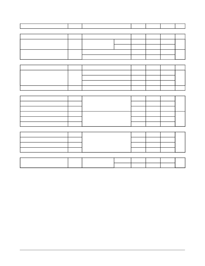
�ELECTRICAL CHARACTERISTIC� S� (T� J� =25� °� C� unless� otherwise� stated)�
�Parameter�
�Symbol�
�Test� Condition�
�Min�
�Typ�
�Max�
�Unit�
�OFF� CHARACTERISTICS�
�Drain� ?� to� ?� Source� Breakdown� Voltage�
�V� (BR)DSS�
�V� GS� =� 0� V,� I� D� =� ?� 250� m� A�
�?� 20�
�V�
�Zero� Gate� Voltage� Drain� Current�
�I� DSS�
�V� GS� =� 0� V,� V� DS� =� ?� 16� V�
�T� J� =� 25� °� C�
�T� J� =� 125� °� C�
�?� 1.0�
�?� 1.0�
�?� 5.0�
�m� A�
�Gate� ?� to� ?� Source� Leakage� Current�
�I� GSS�
�V� DS� =� 0� V,� V� GS� =� ±� 4.5� V�
�0.03�
�1.0�
�m� A�
�ON� CHARACTERISTICS� (Note� 3)�
�V� DS� =� 0� V,� V� GS� =� ±� 12� V�
�6.0�
�Gate� Threshold� Voltage�
�Drain� ?� to� ?� Source� On� Resistance�
�V� GS(TH)�
�R� DS(on)�
�V� GS� =� V� DS� ,� I� D� =� ?� 250� m� A�
�V� GS� =� ?� 4.5� V,� I� D� =� ?� 0.88� A�
�?� 0.45�
�215�
�?� 1.2�
�260�
�V�
�m� W�
�V� GS� =� ?� 2.5� V,� I� D� =� ?� 0.71� A�
�V� GS� =� ?� 1.8� V,� I� D� =� ?� 0.20� A�
�345�
�600�
�500�
�1000�
�Forward� Transconductance�
�g� FS�
�V� DS� =� ?� 10� V,� I� D� =� ?� 0.88� A�
�3.0�
�S�
�CHARGES� AND� CAPACITANCES�
�Input� Capacitance�
�C� ISS�
�155�
�pF�
�Output� Capacitance�
�Reverse� Transfer� Capacitance�
�C� OSS�
�C� RSS�
�V� GS� =� 0� V,� f� =� 1.0� MHz,�
�V� DS� =� ?� 20� V�
�25�
�18�
�Total� Gate� Charge�
�Q� G(TOT)�
�2.2�
�nC�
�Gate� ?� to� ?� Source� Charge�
�Gate� ?� to� ?� Drain� Charge�
�Q� GS�
�Q� GD�
�V� GS� =� ?� 4.5� V,� V� DS� =� ?� 10� V,�
�I� D� =� ?� 0.88� A�
�0.5�
�0.65�
�SWITCHING� CHARACTERISTICS� (Note� 4)�
�Turn� ?� On� Delay� Time�
�t� d(ON)�
�5.8�
�ns�
�Rise� Time�
�Turn� ?� Off� Delay� Time�
�Fall� Time�
�t� r�
�t� d(OFF)�
�t� f�
�V� GS� =� ?� 4.5� V,� V� DD� =� ?� 10� V,�
�I� D� =� ?� 0.5� A,� R� G� =� 20� W�
�6.5�
�13.5�
�3.5�
�DRAIN� ?� SOURCE� DIODE� CHARACTERISTICS�
�Forward� Diode� Voltage�
�V� SD�
�V� GS� =� 0� V,�
�I� S� =� ?� 0.48� A�
�T� J� =� 25� °� C�
�T� J� =� 125� °� C�
�?� 0.8�
�?� 0.66�
�?� 1.2�
�V�
�Product� parametric� performance� is� indicated� in� the� Electrical� Characteristics� for� the� listed� test� conditions,� unless� otherwise� noted.� Product�
�performance� may� not� be� indicated� by� the� Electrical� Characteristics� if� operated� under� different� conditions.�
�3.� Pulse� Test:� pulse� width� ≤� 300� m� s,� duty� cycle� ≤� 2%.�
�4.� Switching� characteristics� are� independent� of� operating� junction� temperatures.�
�http://onsemi.com�
�2�
�发布紧急采购,3分钟左右您将得到回复。
相关PDF资料
NTJD4158CT1G
MOSFET N/P-CHAN COMPL SOT-363
NTJD4401NT1G
MOSFET 2N-CH 20V 630MA SOT-363
NTJD5121NT2G
MOSFET N-CH 60V DUAL ESD SOT363
NTJS3151PT1G
MOSFET P-CH 12V 2.7A SOT-363
NTJS3157NT4G
MOSFET N-CH 20V 3.2A SOT-363
NTJS4151PT1
MOSFET P-CH 20V 3.3A SOT-363
NTJS4160NT1G
MOSFET N-CH 30V 1.8A SC88-6
NTJS4405NT4G
MOSFET N-CH 25V 1A SOT-363
相关代理商/技术参数
NTJD4152PT1G
功能描述:MOSFET 20V 0.88mA P-Channel ESD Protection RoHS:否 制造商:STMicroelectronics 晶体管极性:N-Channel 汲极/源极击穿电压:650 V 闸/源击穿电压:25 V 漏极连续电流:130 A 电阻汲极/源极 RDS(导通):0.014 Ohms 配置:Single 最大工作温度: 安装风格:Through Hole 封装 / 箱体:Max247 封装:Tube
NTJD4158C
制造商:ONSEMI 制造商全称:ON Semiconductor 功能描述:Small Signal MOSFET 30 V/−20 V, +0.25/−0.88 A, Complementary, SC−88
NTJD4158CT1G
功能描述:MOSFET PFET 20V .88A 1OHM RoHS:否 制造商:STMicroelectronics 晶体管极性:N-Channel 汲极/源极击穿电压:650 V 闸/源击穿电压:25 V 漏极连续电流:130 A 电阻汲极/源极 RDS(导通):0.014 Ohms 配置:Single 最大工作温度: 安装风格:Through Hole 封装 / 箱体:Max247 封装:Tube
NTJD4158CT2G
功能描述:MOSFET PFET 20V .88A 1OHM RoHS:否 制造商:STMicroelectronics 晶体管极性:N-Channel 汲极/源极击穿电压:650 V 闸/源击穿电压:25 V 漏极连续电流:130 A 电阻汲极/源极 RDS(导通):0.014 Ohms 配置:Single 最大工作温度: 安装风格:Through Hole 封装 / 箱体:Max247 封装:Tube
NTJD4401N
制造商:ONSEMI 制造商全称:ON Semiconductor 功能描述:Small Signal MOSFET 20 V, Dual N-Channel, SC-88 ESD Protection
NTJD4401N_06
制造商:ONSEMI 制造商全称:ON Semiconductor 功能描述:Small Signal MOSFET 20 V, Dual N-Channel, SC-88 ESD Protection
NTJD4401N_08
制造商:ONSEMI 制造商全称:ON Semiconductor 功能描述:Small Signal MOSFET 20 V, Dual N-Channel, SC-88 ESD Protection
NTJD4401NT1
功能描述:MOSFET 20V Dual N-Channel RoHS:否 制造商:STMicroelectronics 晶体管极性:N-Channel 汲极/源极击穿电压:650 V 闸/源击穿电压:25 V 漏极连续电流:130 A 电阻汲极/源极 RDS(导通):0.014 Ohms 配置:Single 最大工作温度: 安装风格:Through Hole 封装 / 箱体:Max247 封装:Tube